Jump Start Your PCB Adventure
Introduction: Getting started with an electronics project? You need to look into jlc's ecosystem
Today, many hobbyists are learning PCB design to create their own electronic boards. PCBs are more affordable than ever, which motivates many makers to learn PCB design. This wouldn't have been possible even 20 years ago.
My PCB design adventure began in 2019 with an online tutorial. I ordered the PCBs from JLCPCB and the parts from LCSC. JLCPCB had just launched their assembly service, but I still got the parts separately just for the adventure of soldering those smd parts. It was a great experience getting the design become a reality.
If it was the 90s or even the early 2000s, I wouldn't have bothered with PCB design. It was way too expensive, and manufacturers weren't interested in small-time makers like us. It's the same reason we don't really do IC design now - the cost to get a wafer made is crazy high (and that’s not even counting slicing it up and packaging the chips), Selling a kidney might not be enough.
Hopefully, things will change when some fab starts doing prototype orders for hobbyists like us. IC design software has come a long way, so maybe by 2030 we can get our own custom ICs - that would be awesome.
Back to the present: If you're a hobbyist looking to create your own PCBs, it's now possible to design and get them made in under a month. You'll need some basic electronics knowledge and familiarity with components like transistors, resistors, and capacitors. Working with the ICs is no problem - we just refer to the datasheets. Fun fact: I designed my first PCB without even knowing how crystals worked! The point is, you only need to know enough to get started; nobody's an expert right away.
Before diving in, lets familiarize these terms
- EDA - Electronic Design Automation (PCB design software)
- DRC - Design Rule Check
- DFM - Design For Manufacturing
- PCBA - Printed Circuit Board Assembly
- THT - Through Hole Technology
- SMT - Surface Mount Technology
- SMD - Surfact Mount Device
From PCB design to fabrication - here's how you can make it cost-effective and warp-speed your development time.
1) Free Software First

When starting with PCB design, free software is the way to go. EasyEDA (cloud-based) and KiCad (open source) are the best options. For beginners, I recommend EasyEDA due to its user-friendly interface. Once you get the hang of PCB design, you can switch to KiCad or any other software - the core skills will transfer.
I personally use EasyEDA for my open-source projects because its fully integrated with JLCPCB & LCSC, which is where our members usually get our boards. Since the files end up at JLCPCB anyway, I'm not worried about using their cloud storage.
That said, You can also use Kicad - It's a fantastic open-source option that's constantly getting better. And if you like working with JLCPCB, there are some great open-source tools like easyeda2kicad and kicad-jlcpcb-tools to make things easier.
2) Manufacturer Capabilities

When designing a PCB, follow your manufacturer's capacilities (reference: JLCPCB, PCBWay, NextPCB). Set your software's DRC to match these rules; it will then flag any violations.
These specifications generally result in faster production and lower costs:
- FR4 board
- 2,4 layer
- 1.2, 1.6mm board thickness
- Vias 0.3mm or larger, smaller vias increase cost.
- Green color soldermask
3) Start with Hand-Solderable parts

image source: https://core-emt.com/smd-size-chart
When starting with SMD components, choose larger, hand-solderable sizes for easier rework. Avoid packages smaller than 0603 or those with hidden leads like QFNs and BGAs, as these are difficult to rework manually. Once you gain experience, you can move to smaller packages. While smaller components are often slightly cheaper, the difference is negligible for small quantities.
In general, prefer SMD components over through-hole. They are typically less expensive, especially for PCB assembly service.
4) The Cost-Benefit of PCB Assembly

Many manufacturers now offer affordable assembly (PCBA). For example, JLCPCB's assembly cost is only around $8-$25 for 5-10 boards.
- Depending on the complexity of your design, this can save you around 20-60 minutes of soldering time per board. Unless you want to manually reflow them or practice hand-soldering SMDs, just get your boards assembled.
- Double-sided assembly is considerably more expensive, usually costing 2-4 times more; as it adds an extra production step and requires a custom assembly fixture. For most designs, you should be able to pack the parts onto a single side.
- Other than the time-cost benefit, Sometimes getting PCBA can be cheaper than getting the bare boards and components separately. Just look up why some governments have less import tax for Assembled PCB compared to bare PCB - use that to your advantage.
- JLCPCB's ecosystem -
The previous tips were general to all PCB manufacturers. Now we will see how to optimize costs even more, specific to JLCPCB.
- Stick with "Economic" PCBA for prototypes. The "Standard" option is only needed for fine-pitch parts and special components.
- Use components from the JLCPCB parts library, they can be assembled using their PCBA service
- Pick basic/preferred parts for passives since Extended components are charged $3 extra.
As of March 2025, JLCPCB has great deals for 4 and 6 layer prototypes also. That's a great excuse to try it out.
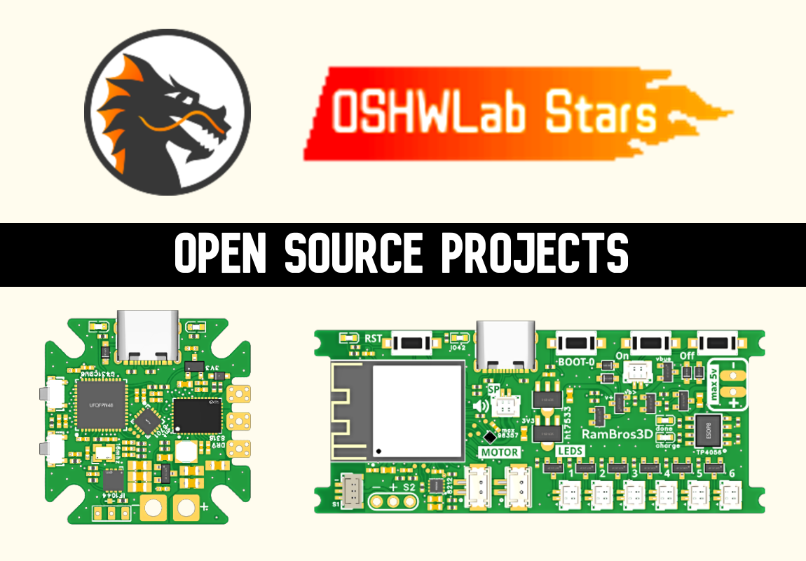
Funding Your Open-Source Hardware:
The OSHWLab Stars initiative offers valuable prototyping support for open-source hardware projects. You can find more details in this article.
Ultimate Advantage:
JLCPCB's access to components from its sister company - LCSC, gives them a significant advantage over competitors, particularly for assembled PCBs. Nowadays bare PCB production is fast across most manufacturers. But Component sourcing time is the bottleneck, it can take an extra 1-3 weeks.
JLCPCB has zero Component sourcing time if you use parts from their library. The whole production (including assembly) typically takes less than a week for 2-6 layer boards.
This highly integrated supply chain allows them to provide the best lead time at the most affordable rates. This allowed them to capitalize on the price elasticity of demand by triggerring substantial demand from hobbyists and small businesses. Like I said before, I wouldnt have gotten into PCB design if it werent for these companies.
- Taking Your Project to Market -
Once you've completed prototyping and built a following, you may find there's demand for your product. What started as a hobby project could become a marketable product. You may not have expected this, but some people will want to buy your product, from you.
Whether you plan to sell bare PCBs, DIY kits, or fully Assembled devices, you'll need to consider additional services like kitting (packaging components together) and subassembly (assembling parts of the product). Also learn about DFM. This journey can be a wild ride, you'll get valuable learning experiences and the potential for a side hustle.
Important considerations:
- I use JLCPCB, so this article is biased in their favor. The focus here is on fast and affordable PCB prototyping. If you have a better alternative, let me know.
- The sales reps from various PCB companies say that their QC is better so they can't match with jlc's prices (for low volume orders), is it true? We will find out.
- Based on the assumption that most hobbyists would be sharing their projects with the community, I have recommended EasyEDA. If you're working on some secret stuff, then I don't have to say the obvious ;)
Article originally published on oshwlab.com